 当前位置:
当前位置: 报告题目: Kelvin probe force microscopy: From atomic scale imaging to application on solar cell materials
报 告 人: Prof. Sascha Sadewasser, International Iberian Nanotechnology Laboratory, Portugal
时 间:2016年9月9日(星期五),上午10:00
地 点:南楼2层会议室
邀 请 人:裘晓辉 研究员(Tel:82545583)
摘要:
To improve understanding of semiconductor materials and device functionality detailed studies are required providing information on materials characteristics on the nanometer scale. Kelvin probe force microscopy (KPFM) is a technique based on non-contact atomic force microscopy (NC-AFM) and is well suited for this task as it measures the surface potential with high spatial resolution. We apply a resonance enhanced mode of operation which allows compensating electrostatic forces using detection ac-voltages below 100 mV; thus, the influence of the KPFM tip on the semiconductor is minimized [1].
This talk will first introduce the KPFM method. It will then be demonstrated that for correct height imaging the KPFM method is superior to regular NC-AFM. Depending on the sample bias, even a contrast inversion can be observed in regular NC-AFM topography imaging [2]. On the Si(111) 7x7 surface, atomic scale contrast in the contact potential is observed, which is explained by short range electrostatic forces due to an induced dipole in the surface [3]. For the application to chalcopyrite semiconductors (i.e. Cu(In, Ga)Se2) in thin film solar cells, it is shown that differently oriented facets of single semiconductor grains show a distinct work function [4]. The investigation of grain boundaries in these polycrystalline thin films shows a local band bending due to the presence of charges [5]. However, for an epitaxially grown S3 grain boundary, a charge neutral barrier to majority transport could be identified for CuGaSe2 [6].
[1] Ch. Sommerhalter et al., Appl. Phys. Lett. 75, 286 (1999).
[2] S. Sadewasser et al., Phys. Rev. Lett. 91, 266101 (2003).
[3] S. Sadewasser et al., Phys. Rev. Lett. 103, 266103 (2009).
[4] S. Sadewasser et al., Appl. Phys. Lett. 80, 2979 (2002).
[5] D. Fuertes Marrón et al., Phys. Rev. B 71, 033306 (2005).
[6] S. Siebentritt et al., Phys. Rev. Lett. 97, 146601 (2006).
|
|
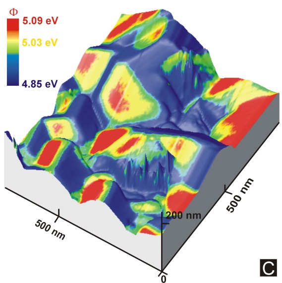
KPFM measurement of a CuGaSe2 thin film grown on a single crystalline ZnSe(110) substrate. The 3-dimensional effect shows the topography, while the coloring provides the simultaneously measured work function. Different facets of grains show constant but distinct work function, due to an orientation dependent surface dipole [4].
|
报告人简介:
Sascha Sadewasser holds a Dipoma (1995) in Physics from the RWTH Aachen, Germany and a PhD (1999) from the Washington University St. Louis, MO, USA. For both degrees he worked on high temperature superconductors. As a post doctoral researcher he stayed for 4 years (1999-2003) at the Hahn-Meitner Institute Berlin, where he worked on the nanoscale characterization of semiconductor materials for thin film solar cells using scanning probe microscopy methods. As a Ramón y Cajal scientist he joined the Centro Nacional de Microelectonica in Barcelona, Spain from 2003 to 2004, where he worked on the fabrication of nano- and micro-electromechanical systems (NEMS and MEMS). From 2005 until 2011 he was the group leader of the Nanoanalytics and Nanofabrication group at the Helmholtz-Zentrum Berlin, Germany and the deputy head (2008-2011) of the Department for Heterogeneous Materialsystems, working with scanning probe microscopy and on the nanostructured materials growth of Cu(In,Ga)Se2 semiconductors for solar cell applications. In 2011 he obtained his Habilitation in Experimental Physics from the Free University of Berlin, Germany.
In July 2011 he started as the group leader of the Laboratory for Nanostructured Solar Cells (LaNaSc) at the INL - International Iberian Nanotechnology Laboratory, where his research will be focused on the development of chalcopyrite-type quantum dots for solar cells and their characterization using scanning probe microscopy.
| 相关附件 |
|---|
| 相关文档 |
|---|
 版权所有@中国科学院纳米标准与检测重点实验室
 联系方式:北京市海淀区中关村北一条11号(100190) 电话:010-82545691 传真:010-62656765
E-mail: baoxf@nanoctr.cn